2 nm

Samsung Elect
2026-09-07 02:09:06

Samsung and Arm said to be developing a 2 nm on-device AI chip, with OpenAI rumored as a possible customer

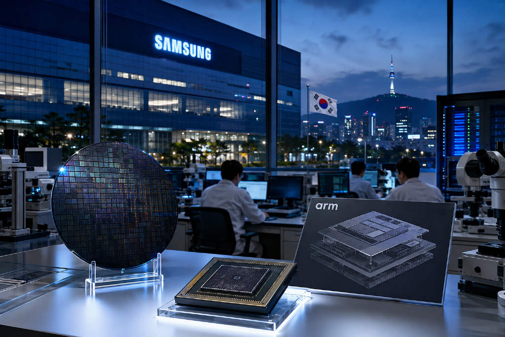
Samsung Electronics and Arm are reportedly working together on a next-generation AI chip built on Samsung’s 2 nm gate-all-around (GAA) process, according to reports cited by ABMedia from outlets including TradingKey. The project is focused on a system-on-chip for on-device AI, and Arm reportedly approved the non-recurring engineering, or NRE, cost for the program in late August, marking the formal start of joint development. The reported division of work gives Arm responsibility for the AI accelerator architecture and register-transfer level design. Samsung’s System LSI unit is said to be handling SoC design and integration using Arm’s IP, while Samsung Foundry would take charge of manufacturing, advanced packaging, and commercialization. For Samsung Foundry, the project is framed as an important step in winning a flagship customer at the 2 nm node. One of the main questions around the project is the end customer. Industry sources cited in the report said OpenAI is a candidate, but Arm, Samsung, and OpenAI have not confirmed that claim. ABMedia also noted that Samsung has recently been active in custom AI chip efforts, and that earlier reporting had linked Anthropic with discussions around a custom 2 nm AI chip with Samsung.
20
Samsung and Arm said to be developing a 2 nm on-device AI chip, with OpenAI rumored as a possible customer
Intel
2026-08-20 03:58:48

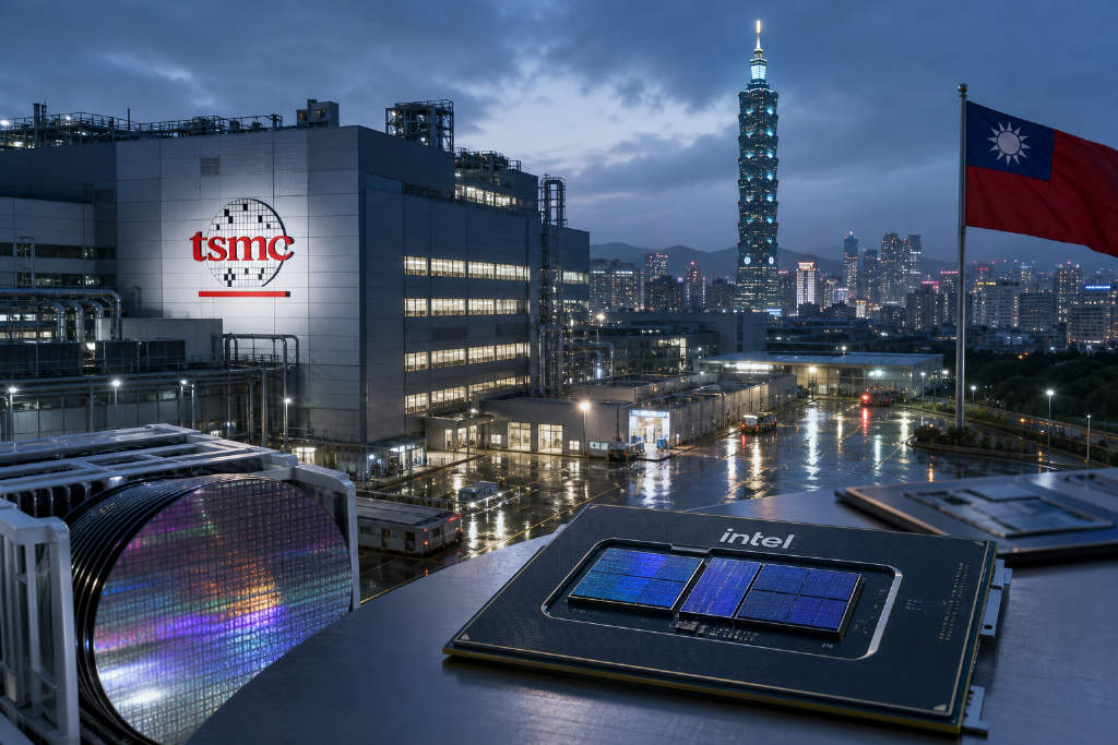
Intel’s next PC chips are said to expand TSMC 2 nm use as supply-chain names come into view

ABMedia, citing Commercial Times, reported that Intel’s next-generation PC processor roadmap could deepen its reliance on Taiwan Semiconductor Manufacturing Co. across the full 2 nm family. The report said Nova Lake desktop chips are expected to use a hybrid process approach combining Intel 18A with TSMC N2P, while Razor Lake may move further to TSMC N2X, a higher-performance extension of the N2 platform aimed at high-frequency CPU, AI and HPC workloads. Supply-chain sources also said Nova Lake desktop parts may be the first to introduce bLLC, or Big Last-Level Cache, with notebook adoption possibly deferred to the later Razor Lake-HX generation. The article also highlighted a strategic reading from Citrini analyst Jukan, who argued that Intel’s TSMC allocation should not be viewed only as a response to concerns around Intel 18A yields. In his view, maintaining or expanding wafer capacity at TSMC could also limit the room available to AMD for server CPU production, putting pressure on AMD’s shipment timing, scale and expansion pace. On the supplier side, the report named Taiwanese companies such as Phoenix Silicon International and Chung-Hsin Electric & Machinery-linked China Sand, saying tighter process requirements at 2 nm and 1.6 nm are lifting demand for CMP-related materials and tools.

340
Intel’s next PC chips are said to expand TSMC 2 nm use as supply-chain names come into view
TSMC
2026-08-19 04:53:59

TSMC validates A16 backside power platform as NVIDIA lines up Feynman on the node

TSMC has completed development and validation of its A16 process platform built with Super Power Rail, or SPR, a backside power delivery network that ETNews said preserves compatibility with existing design ecosystems. The report says TSMC is the first foundry to bring backside power supply technology to the Angstrom-class era while keeping current design infrastructure largely intact, a point that matters for large chip customers already invested in the N2 and N2P ecosystem. According to the report, the move addresses a growing bottleneck in sub-2 nm chip design, where power and signal routing compete for limited front-side space, raising routing congestion and voltage drop risks. TSMC’s SPR architecture shifts power delivery to the back of the chip and uses dedicated backside contacts to feed each transistor’s source and drain, while leaving front-side gate structures, cell size, and layout area nearly unchanged. ETNews said A16 can deliver 8% to 10% higher performance at the same power, or cut power use by 15% to 20% at the same speed, with chip density also rising 8% to 10% versus N2P. The report also said NVIDIA’s next-generation AI accelerator platform, Feynman, will use A16 and aims for mass production in the second half of 2028, alongside large-scale use of CPO and SoIC 3D stacking.

600
TSMC validates A16 backside power platform as NVIDIA lines up Feynman on the node
NVIDIA
2026-08-14 04:15:14

NVIDIA’s Feynman platform is said to target TSMC A16 and large-scale CPO deployment in 2028

NVIDIA has already moved into development and supply-chain planning for Feynman, the AI accelerator platform expected to follow Rubin, according to a Digitimes report cited by ABMedia. The report says Feynman is set to use TSMC’s upgraded A16 process, pair it with custom HBM, and adopt both SoIC 3D stacking and co-packaged optics, or CPO, at scale, with volume production targeted for the second half of 2028. What makes the platform notable is the simultaneous push across three technical layers: process technology, advanced packaging, and optical interconnect. Supply-chain data cited in the report shows NVLink bandwidth rising from about 130 TB/s in Blackwell NVL72 racks to 260 TB/s in Rubin, 520 TB/s in Rubin Ultra, and more than 1,000 TB/s in Feynman. At that level, copper links are approaching practical limits in distance, power, signal loss, and thermal management, making optical interconnect a more direct fit for large AI clusters. The same report says TSMC is expanding advanced packaging capacity from AP5 and AP6 into AP7 and AP8, while repeatedly lifting SoIC monthly capacity targets from 20,000 wafers by the end of 2026 to 50,000 by the end of 2027. It also places Feynman inside NVIDIA’s wider capital and supply strategy, including more than $40 billion invested across the AI ecosystem since 2026 and a financing platform with Apollo, BlackRock, Blackstone, and Goldman Sachs aimed at mobilizing $500 billion in third-party capital.

1170
NVIDIA’s Feynman platform is said to target TSMC A16 and large-scale CPO deployment in 2028
Elon Musk
2026-08-12 12:25:08

Musk’s TeraFab fuels new scrutiny of FEL as a possible lithography challenger

Elon Musk’s TeraFab chip manufacturing plan has moved from a compute-supply story into a lithography debate after speculation that the project may be aligned with a free-electron laser, or FEL, approach to extreme ultraviolet light sources. The discussion gained momentum after Musk posted 「FEL FTW」 on social media, a remark that many read as support for the idea. The core issue is whether FEL can attack one of the most entrenched positions in the semiconductor equipment business: ASML’s dominance in EUV lithography. The article lays out why that question is drawing attention now. ASML’s laser-produced plasma, or LPP, light source enabled commercial EUV, but its limits are becoming more visible as the industry pushes toward 2 nm and below. Conversion efficiency remains low, tin debris contaminates costly mirrors, and power requirements keep rising. FEL backers argue their approach avoids plasma conversion, removes tin-droplet contamination, and could deliver much higher EUV output. xLight, which raised an oversubscribed $40 million Series B in July last year and later brought in former Intel CEO Pat Gelsinger as executive chairman, says its system could sharply raise fab productivity. Even so, the broader field remains mixed. ASML is still expanding EUV and DUV output, advancing High-NA EUV, and posting rising sales and profit. At the same time, alternative paths including X-ray lithography, nanoimprint lithography, and electron-beam direct write are also developing, each with different trade-offs in cost, throughput, and manufacturability.

3500
Musk’s TeraFab fuels new scrutiny of FEL as a possible lithography challenger
TSMC
2026-08-10 03:22:03

Longtan science park expansion restarts as TSMC signals interest in 1.4 nm fabs

The long-delayed third-phase expansion of the Longtan Science Park has been revived after more than two years of setbacks tied to land expropriation disputes. According to ABMedia, citing a Liberty Times report, local sentiment in Longtan shifted after residents saw the economic spillover created by Taiwan Semiconductor Manufacturing Co. (TSMC) plants in southern Taiwan, including Tainan, Kaohsiung, and Chiayi. Supply chain sources said TSMC is planning three facilities for the site: two 1.4 nm wafer fabs and one panel-level packaging, or PLP, plant. The project was originally designed to cover 158.59 hectares, with 88% of the land privately owned, triggering strong opposition and organized protests. TSMC later announced on Oct. 17, 2023 that it would abandon its Longtan plant plan. Since then, the project scope has been revised several times, first to 89.63 hectares in 2024 and later to 104.19 hectares, of which about 46 hectares are designated for industrial use. Taiwan’s National Science and Technology Council said the expansion plan passed review by the Science Park Review Committee in May and was submitted to the Executive Yuan in June. Under the current timetable, land acquisition is targeted for completion by the end of 2029, with public infrastructure construction scheduled to begin in 2030.

1400
Longtan science park expansion restarts as TSMC signals interest in 1.4 nm fabs
Fujian Jinhua
2026-08-05 12:29:20

Fujian Jinhua and CXMT started in the same year. A decade later, their paths split sharply

ChangXin Memory Technologies’ listing has pushed China’s DRAM industry back into the spotlight, but the attention has also revived comparisons with another project launched in 2016: Fujian Jinhua Integrated Circuit Co. Both companies were created to break China’s dependence on foreign DRAM suppliers. Both planned 12-inch wafer fabs. Both drew investment measured in the hundreds of billions of yuan. Yet their outcomes diverged dramatically. Fujian Jinhua moved quickly at the start, signing a May 2016 cooperation agreement with United Microelectronics Corp. under which Jinhua would fund and build a 12-inch fab while UMC developed a 32 nm DRAM process. The first phase of the Jinjiang project carried planned investment of about RMB 37 billion, targeted mass production in 2018, and was designed for monthly capacity of 60,000 wafers. But in 2017, Micron sued UMC and Fujian Jinhua in Taiwan and the United States, alleging trade secret theft and patent infringement. The dispute escalated in October 2018, when the U.S. Commerce Department placed Fujian Jinhua on the Entity List, triggering a broad halt in equipment, software, and technical support. The legal fight dragged on for about six years. By the time a U.S. federal court in Northern California ruled in February 2024 that prosecutors had failed to prove Fujian Jinhua stole Micron trade secrets, the company had already missed the industry upcycle that later helped CXMT expand and reach the capital market. The comparison highlights differences in IP strategy, supply-chain resilience, and timing in China’s memory-chip push.

1960
Fujian Jinhua and CXMT started in the same year. A decade later, their paths split sharply
China lithogr
2026-07-28 02:11:00

China-made immersion DUV tools move into pilot production, but the gap with ASML remains wide

A PANews article argues that recent reports around China-made immersion deep ultraviolet lithography systems should be read with caution, not as proof that China has cracked the lithography bottleneck or entered a “DeepSeek moment” for chipmaking equipment. According to the piece, a state-backed company in Shanghai has begun small-batch production of domestic immersion DUV tools, with about five units planned this year for Semiconductor Manufacturing International Corp. (SMIC), Hua Hong Semiconductor, and ChangXin Memory Technologies, and a target of roughly 20 units in 2027. The article says the development matters because it appears to move domestic immersion DUV systems from R&D and prototype validation into initial production and customer introduction. At the same time, it stresses that public information does not yet prove the machines have passed fab acceptance or can run at full commercial standards over long periods. It also questions widely circulated figures such as support for 28 nm, localization above 85%, and yield above 90%, noting that no full testing reports or statistical definitions have been publicly disclosed. The piece draws a sharp line between DUV and EUV. Progress in immersion DUV could help China strengthen supply security for mature and some advanced nodes, but it does not mean EUV challenges have been solved. For investors, the article says the real checkpoints over the next few years will be fab acceptance, uptime, throughput, overlay precision, defect stability, repeat orders, and the domestic substitution rate of key components.

1600
China-made immersion DUV tools move into pilot production, but the gap with ASML remains wide